Components | One article takes you through the concept of "field-effect transistors" in electronic components
Field-effect transistor
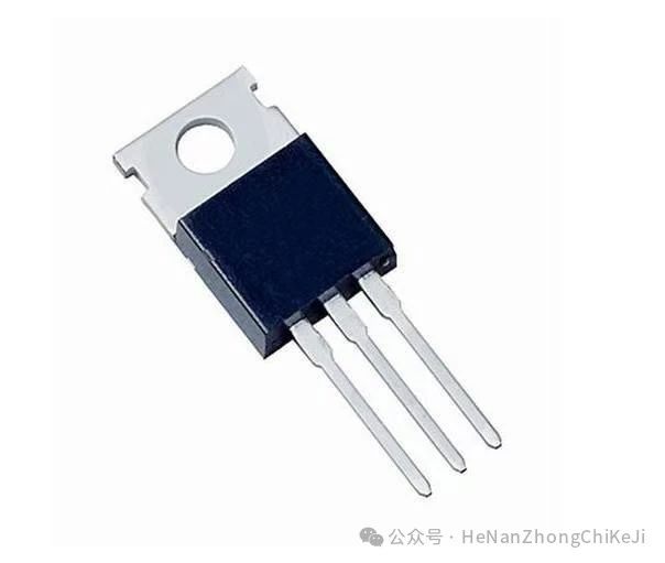
1、 Introduction to Field Effect Transistor (FET)
2、 The working principle of FET
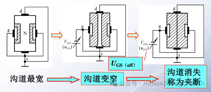
Field effect transistors are mainly composed of three regions: gate, drain, and source. In normal operating conditions, the gate voltage controls the current between the source and drain, thereby achieving control over the field-effect transistor.
Cut off state: When the gate voltage is lower than the threshold voltage, there is no conductive channel between the gate and the channel, and electrons cannot flow from the drain to the source. The field-effect transistor is in a cut off state, equivalent to an insulator.
Conductive state: When the gate voltage is higher than the threshold voltage, a conductive channel is formed between the gate and the channel, and electrons can flow from the drain to the source along the channel. At this point, the carrier concentration near the source increases, forming a conductive region called the inversion layer (N-type or P-type).
Enhanced conductivity: As the source voltage further increases, the width of the inversion layer will increase, and the electron concentration in the channel will also increase. In this way, more electrons can flow from the drain to the source, forming a conductive channel. When the source voltage reaches a certain value, the electron concentration in the channel is high enough to make the entire channel conductive.
Fully conductive: When the gate voltage is 0V, due to the disappearance of the insulation layer between the gate and channel, electrons in the channel can freely flow between the drain and source. This means that the field-effect transistor is in a conducting state.
3、 The main types of FET
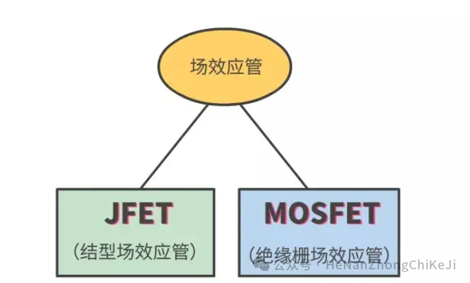
(1) Junction Field Effect Transistor (JFET):
JFET uses PN junction as gate control, with PN structures on both sides sandwiching a channel region.
By changing the bias of the PN junction between the gate and channel, the width of the channel can be controlled, thereby controlling the current between the drain and source.
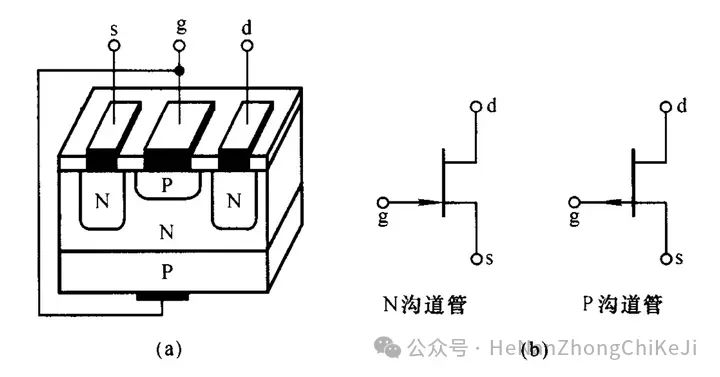
Application scenarios: JFETs are commonly used in high input impedance circuits, signal amplifiers, and electronic switches.
(2) Insulated Gate Field Effect Transistor (MOSFET):
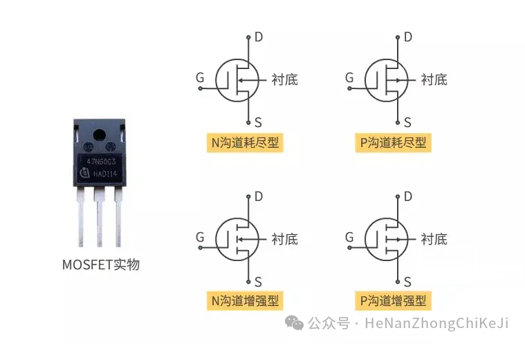
MOSFET consists of a metal gate, an oxide insulation layer, and a semiconductor channel, with the gate and channel isolated by an insulation layer.
The change in gate voltage will induce charges on the insulating layer, forming or enhancing a channel, thereby controlling the current between the drain and source.
Structural characteristics
Application scenarios: MOSFETs are widely used in fields such as digital circuits, analog circuits, power management, and RF amplification.
Gate (G): The control terminal of MOSFET, which controls the formation of the channel by changing the gate voltage, thereby controlling the current between the drain and source.

Amplifier: Utilizing high input impedance characteristics for signal amplification.
Electronic switch: fast switching capability, suitable for electronic switch applications.
Power management: controls power flow for power converters and regulators.
Digital circuits: Building logic gates and other digital circuits.
High input impedance: FET has a very high input impedance, which has little impact on the front-end circuit.
Low noise: suitable for high fidelity audio applications, providing clear signals.
Quick response: suitable for high-frequency applications.
Set the gate voltage correctly to ensure that the FET operates in the appropriate state.
Pay attention to thermal management to avoid overheating of components.
Take appropriate electrostatic discharge (ESD) protection measures.

推薦
-

-

QQ空間
-

新浪微博
-

人人網
-

豆瓣

